Reduce Electronic Device Shock and Vibration Testing Cost and Time via Mechanical Analysis
Summary
Finite element analysis (FEA) can simulate military shock and vibration testing on electronic components before physical prototypes are built. In this case study, engineers analyzed a printed circuit board (PCB) power supply using FEA to successfully reduce the cost and risk of meeting MIL-S-901D shock and MIL-S-167 vibration testing. The simulation identified high-stress areas in component leads and solder joints, allowing engineers to modify the design and significantly reduce failure risk before manufacturing and testing.
Why Was Finite Element Analysis (FEA) Used for PCB Shock and Vibration Analysis?
A commercial-off-the-shelf power supply was being modified for military applications to fill a critical need on a short time frame. However, it was still required to comply with strict the US Navy’s shock and vibration testing standards.
Before manufacturing costly prototypes, engineers needed to determine whether the existing design could withstand:
• MIL S 901D shock testing
• MIL S 167 vibration testing
To reduce development risk and cost, engineers used FEA to simulate the required testing conditions and identify potential structural weaknesses in the printed circuit board (PCB). This approach allowed design improvements to be made before physical testing and production.
How Was Finite Element Analysis Applied to the Printed Circuit Board?
To accurately evaluate the PCB’s structural response, engineers created detailed three-dimensional finite element models of the circuit boards.
The FEA models included:
- The printed circuit board structure
- Major electrical components
- Mounting screws and attachment points
- Component wires and electrical leads
- Detailed solder joint connections
Particular attention was paid to solder joints, which are often critical failure points during vibration and shock loading. The simulation models were developed using PTC Pro/ENGINEER (now Creo Parametric) for CAD modeling and ANSYS Multiphysics for structural analysis (Figures 1 and 2).
 Figure 1: Example FEA natural frequency mode shape of a similar non-confidential PCB.
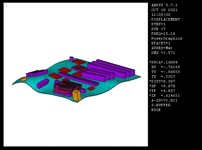
Figure 2: The FEA program outputs modal analysis animations to help ensure there are no excitation sources near lightly damped natural frequency modes.
How Were Military Shock and Vibration Conditions Simulated?
To replicate real-world operating conditions, engineers applied the same loading conditions required by military testing protocols.
Random Vibration Testing Simulation
Random vibration loads were applied to the PCB through the mounting points on the rack to simulate Environmental Stress Screening (ESS) conditions.
Multi-Direction Shock and Vibration Loading
Shock and vibration loads were applied separately in three orthogonal directions to comply with military testing specifications. The simulations evaluated:
- Component deflection
- Stress levels in solder joints
- Structural behavior during shock events
- Natural frequency mode shapes
Animated visualizations were generated to illustrate both modal vibration behavior and transient shock response.
What Problems Were Identified During the Analysis?
The FEA simulation revealed that several component leads and solder connections experienced elevated stress levels during the simulated shock and vibration events.
These locations were identified as potential failure points during physical testing.
The animated deflection plots clearly showed that some electronic components were experiencing “tipping” motion (Figure 3), which increased stress on the leads and solder joints.
 Figure 3: Deformation and high stress locations were identified during simulated shock events. MSI worked with the PCB manufacturer’s engineers to iterate and re-analyze a successful design that met physical testing requirements.
How Was the PCB Design Improved?
Based on insights from the simulation results, MSI worked with the PCB manufacturer’s engineers to successfully modify the PCB design to improve structural stability.
Key Design Improvements
The primary solution was to add additional structural support to the components to prevent tipping motions during vibration. After implementing the design changes, the PCB was reanalyzed using FEA simulations.
Results showed:
- Significantly reduced stress levels
- Improved structural stability
- Lower risk of solder joint failure during testing
This design optimization increased the likelihood that the power supply would successfully pass military shock and vibration qualification testing.
Why Is Finite Element Analysis Valuable for Electronics Reliability Testing?
Complex three-dimensional simulations like these are often perceived as time-consuming. However, by combining efficient CAD modeling tools with advanced simulation software, engineers were able to perform the analysis quickly while maintaining a high level of detail.
Benefits of using FEA for electronics testing include:
- Identifying failure risks before prototype manufacturing
- Reducing development time and cost
- Improving product reliability
- Supporting compliance with military testing standards
- Providing visual insight into vibration behavior
- Reputation protection
Learn More About Shock and Vibration Analysis
For more insights into electronics reliability and structural analysis, explore additional resources on shock testing simulation for electronic components and related engineering case studies.
You may also be interested in our circuit board thermal analysis case study, which examines thermal stresses and reliability in electronic systems.
Frequently Asked Question
What are common PCB failure points?
Typical failure points include:
• Solder joints
• Component leads
• Mounting connections
• Flexible components
What is shock and vibration analysis and testing for PCBs?
Shock and vibration analysis evaluates whether a printed circuit board can withstand mechanical loads encountered during transportation, operation, or military environments. Testing is used to demonstrated that shock and vibration requirements are met.
Why is FEA used prior to PCB testing?
To save time and money. FEA allows engineers to simulate shock and vibration conditions digitally, helping identify weak points such as solder joints and component leads before prototypes are built and tested.
What military standards apply to shock and vibration testing?
Common military standards include MIL‑S‑901D for shock testing and MIL‑S‑167 for vibration testing of shipboard equipment.
How does FEA improve electronics reliability?
Finite element analysis helps engineers detect structural weaknesses, optimize component support, and ensure electronic systems meet environmental testing requirements.
